Note: This article discusses the material principles, manufacturing processes, defect transmission mechanisms, and evaluation methods of C19400 lead frame copper strips. It does not provide directly reproducible parameters for melting compensation, hot rolling temperature, cold rolling reduction ratio, annealing schedules, etching solution formulations, or electroplating parameters. Copper strips of the same grade used for stamping, etching, and pre-plating applications may have different microstructures, surface conditions, residual stresses, and delivery states.
Inside a molded semiconductor package, the component that truly supports the chip, connects external leads, and transfers heat from the chip to the outside is not only the bonding wire. Beneath the chip lies a thin and highly precise metal framework—the lead frame. It must withstand die bonding, wire bonding, encapsulation, reflow soldering, trimming and forming, as well as long-term thermal cycling. Therefore, it serves not only as a conductor but also as a structural support, heat dissipation pathway, and dimensional reference.
C19400 is one of the most representative Cu–Fe–P lead frame copper alloys. It typically contains approximately 2.1%–2.6% Fe, small amounts of P and Zn, with the balance being Cu. Official material data positions it as an electronic copper alloy that combines medium strength, relatively high electrical conductivity, good stress relaxation performance, stamping capability, etching adaptability, and electroplating compatibility [1-7].
However, producing a qualified coil of C19400 copper strip is far more complex than simply rolling a copper alloy down to a thickness of 0.1–0.3 mm. Lead frame manufacturing requires simultaneous control of thickness, flatness, residual stress, strength, electrical conductivity, grain structure, second phases, surface quality, and slitting edge conditions across hundreds of millimeters of strip width and thousands of meters of coil length. Any localized defect can be amplified during subsequent stamping or etching processes.
The true value delivered by lead frame copper strip is not merely a material grade, but a precision strip capable of consistently passing stamping, etching, plating, wire bonding, and molding processes.
1. What Functions Does a Lead Frame Perform Inside a Chip?
Lead frames are positioned between the bare semiconductor die, bonding wires, the molded encapsulation, and the external circuit, serving four primary functions:
Mechanical support: Secure the die and wire bonding area while withstanding the stresses of die attach, wire bonding, molding compound flow, and trim-and-form processes.
Electrical interconnection: Transfer electrical signals and current from the chip bonding pads to the external package leads.
Thermal dissipation: Conduct heat away from the chip through the die pad and leads to the package body, PCB, or external heat dissipation structures.
Dimensional accuracy: Ensure precise lead pitch, coplanarity, positional accuracy, and assembly consistency.
Lead frames are widely used in QFN, QFP, SOP, power discrete devices, LEDs, sensors, analog ICs, and automotive electronic packages. For power semiconductor devices, the lead frame serves as the primary pathway for both electrical current and heat transfer. For fine-pitch logic devices, greater emphasis is placed on etching precision, lead straightness, and surface quality to ensure reliable package performance.
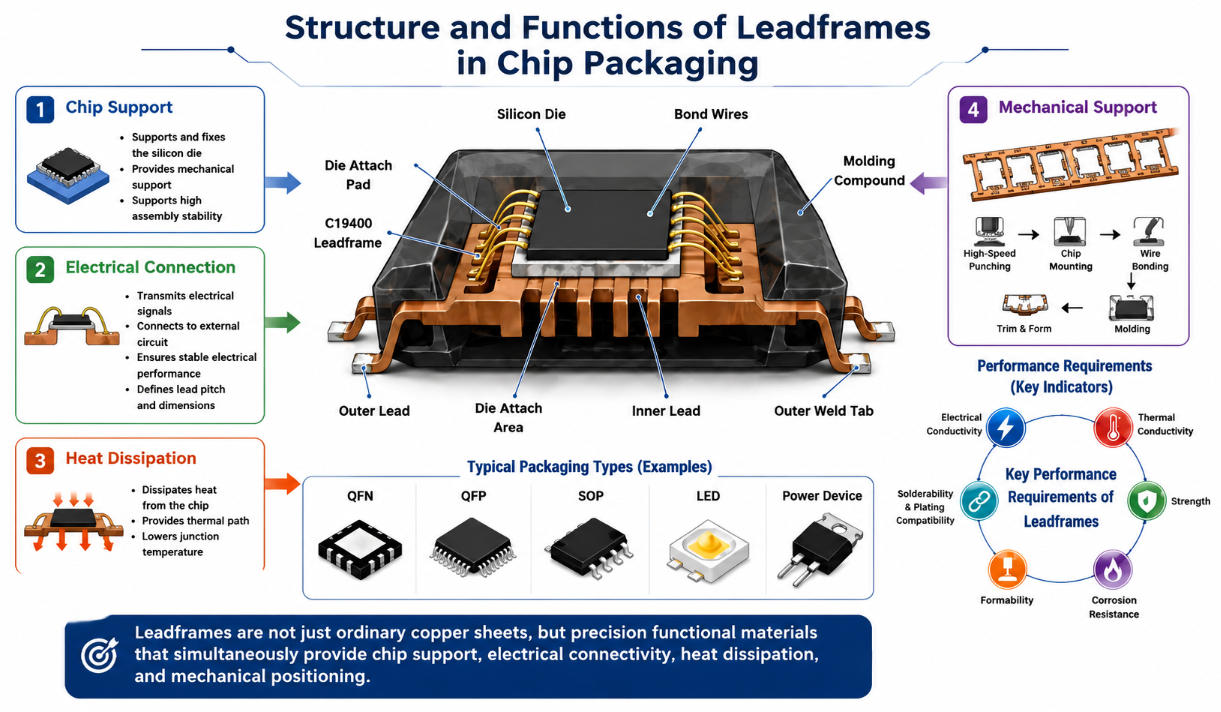
Figure 1. Structure and functions of a lead frame in semiconductor packaging
2. Why Not Directly Use Pure Copper Strip?
Pure copper offers higher electrical conductivity and thermal conductivity, but its strength, resistance to softening, and dimensional stability are insufficient for thin strips. During high-speed stamping, leads may experience bending, collapse, and feeding deformation. After package reflow and thermal cycling, residual stress and stress relaxation may further affect coplanarity.
C19400 improves the copper matrix through Fe-based dispersed particles, cold working, and grain boundary strengthening, while minimizing electron scattering caused by alloying elements. Product data from KME, Aurubis, Proterial, and Mitsubishi all describe C19400 as a balanced electronic copper alloy featuring “medium strength + relatively high conductivity + good stress relaxation, stamping, etching, and plating performance” [3-7].
| Material System | Electrical Conductivity Level | Strength Level | Stress Relaxation | Processing Characteristics | Typical Positioning |
|---|
| Pure copper | Highest | Low | Weak | Easy to process, but limited thin-strip rigidity and thermal stability | High thermal conductivity components under low load |
| C19400/CuFe2P | High | Medium | Good | Balanced performance in stamping, etching, plating, and cost | General lead frames and connectors |
| Cu-Ni-Si alloys | Medium-high | Higher | Better | More complex heat treatment and surface control, higher cost | High-strength, high-reliability lead frames |
Therefore, C19400 is not the highest-performance material among all lead frame alloys. Instead, it occupies the long-term balance zone between cost, strength, conductivity, surface processing capability, and mass production stability.
3. Complete Manufacturing Route of C19400 Copper Strip
Raw material preparation and melting → Ingot casting or continuous casting → Surface milling → Hot rolling → Multi-pass cold rolling → Intermediate annealing / precipitation control → Final rolling → Tension leveling → Cleaning and surface control → Slitting and packaging → Stamping or etching → Electroplating and package validation
ASTM B465 requires C19400 plate, strip, and sheet materials to start from dense cast blanks suitable for hot working, cold working, and annealing, and ultimately achieve a uniform deformation structure [2]. In actual production lines, ingot casting routes, horizontal continuous casting routes, and continuous casting and rolling routes may all be adopted. However, all routes must ultimately undergo multi-stage rolling and heat treatment processes.
The manufacturing sequence determines the material condition. Hot rolling is responsible for breaking down the cast structure and forming the strip slab. Cold rolling increases strength, controls thickness and flatness. Annealing releases residual stress, regulates recrystallization and precipitation behavior. Final rolling and tension leveling determine the final dimensions, flatness, and feeding stability.
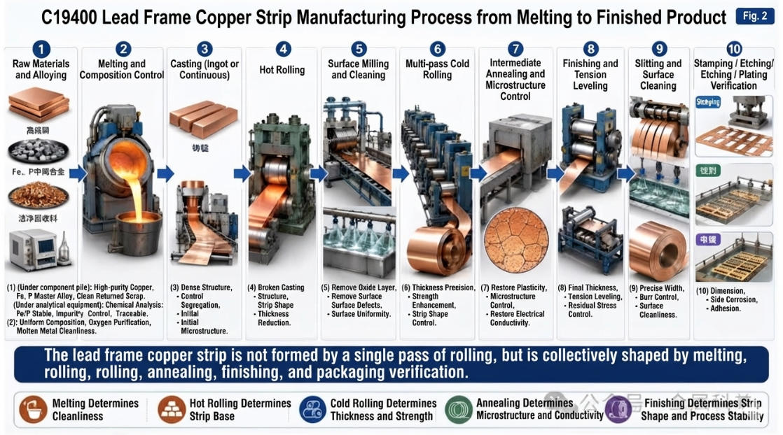
Figure 2. Manufacturing route of C19400 lead frame copper strip from melting to finished product
4. Melting and Casting: Meeting Average Composition Requirements Does Not Mean Microstructural Cleanliness
Although the alloying element content of C19400 is not high, the ratio of Fe, P, and Zn affects precipitation phases, electrical conductivity, and hot working behavior. If Fe content is too low, strengthening is insufficient; if Fe content is too high or solidification segregation is severe, coarse Fe-rich particles may form. P can form compound phases with Fe and help control matrix solutes, but excessive P can also reduce electrical conductivity and alter hot-working plasticity.
Key factors controlled during this stage include:
Stability of Fe, P, Zn, and major impurity contents between different melting batches;
Oxide inclusions, slag, and unmelted master alloy particles;
Shrinkage cavities, center porosity, surface cracks, and head-to-tail segregation;
Coarse Fe-rich/Fe-P particles and their spatial distribution;
Sources of recycled materials, coatings, and contamination from other alloying elements.
Coarse particles in the as-cast structure may be crushed, elongated, or arranged into stringers during rolling, but they do not necessarily dissolve completely. These particles may later cause hard spots, burrs, and abnormal tool wear during stamping, or create local differences in etching rates.
5. Hot Rolling and Surface Milling: Transforming Cast Ingots into Slabs Suitable for Precision Cold Rolling
Cast ingots usually require removal of defective zones and surface milling to eliminate oxide scale, segregation layers, and casting surface defects. If the defective surface layer is not sufficiently removed, surface cracks may be pressed into the interior of the copper strip during subsequent cold rolling, forming linear defects.
The primary purpose of hot rolling is to compact porosity, break down cast grains and coarse particles, and transform the ingot into a hot-rolled strip slab with relatively uniform thickness. Meanwhile, temperature and strain conditions differ between the surface, center, and edges, which may create microstructural gradients and residual stress differences.
After hot rolling, attention should be paid to surface oxidation, edge cracking, center defects, slab thickness variation, and banding of Fe-rich particles. Since lead frame copper strips are later reduced to very thin gauges, defects that are barely visible at the early stage may be elongated into continuous defects extending several meters or even longer after multiple thickness reductions.
6. Cold Rolling: The Core of the Process Is Not Simply “Reducing Thickness,” but Reducing Thickness Stably
Cold rolling simultaneously changes thickness, surface condition, strength, texture, residual stress, and subsequent etching behavior. After cold rolling, C19400 copper experiences increased dislocation density and deformation texture, resulting in higher strength. However, longitudinal, transverse residual stresses, and anisotropy within the strip also increase significantly [10-15].
Lead frame copper strips require control of:
Longitudinal and transverse thickness variation, as well as thickness stability from head to middle to tail;
Center waves, edge waves, camber, twisting, and warpage after slitting;
Work roll marks, scratches, dents, and surface roughness;
Work hardening, elongation, and bending performance;
Residual stress and deformation after subsequent etching.
Research shows that the strength and residual stress of cold-rolled Cu–Fe–P strips are significantly higher than those of hot-rolled or annealed materials. Appropriate recrystallization, reduction of dislocation density, and texture adjustment can reduce residual stress while maintaining sufficient strength [10-14].
This is why lead frame copper strips cannot be described only by terms such as “hard state” or “semi-hard state.” The same hardness value may result from different combinations of dislocations, grain structure, precipitation, and residual stress, leading to different stamping and etching performance.
7. Annealing and Precipitation: Neither Softer nor Harder Is Always Better
The microstructural control of C19400 relies on the combined effects of cold working, recovery and recrystallization, and Fe-based precipitation. Short-term annealing studies show that increasing temperature leads to reduced dislocation density, texture changes, residual stress relaxation, and local recrystallization. However, excessive annealing may reduce strength and cause grain coarsening, resulting in insufficient stiffness of thin leads [11-13].
| Condition | Microstructural Characteristics | Possible Performance Effects |
|---|
| Insufficient cold rolling / Excessive annealing | Low dislocation density, high recrystallization ratio, relatively coarse grains | Insufficient strength, reduced lead rigidity and feeding stability |
| Proper thermomechanical condition | Fine Fe-based particles + moderate dislocation density + controlled grain size and texture | Balanced strength, conductivity, flatness, and formability |
| Excessive cold rolling / Insufficient annealing | High dislocation density, strong deformation texture, high residual stress | Increased risk of etching warpage, bending cracks, and slitting deformation |
Fe-based particles can both hinder dislocation movement and grain boundary migration while also affecting etching and surface reactions. When particle size, density, and distribution are uneven, the material may experience localized hard spots, residual stress gradients, and differences in etching rates [15-18].
8. Tension Leveling and Slitting: Why Do Flatness Problems Often Appear at the Final Stage?
Even after final rolling, copper strips that meet thickness requirements may still contain edge elongation, center elongation, and potential residual stress. Tension leveling uses stretching and repeated small bending processes to redistribute stress, allowing the copper strip to maintain flatness under free conditions.
However, leveling is not simply a matter of “straightening.” Insufficient leveling may cause feeding deviation during high-speed stamping. Excessive leveling may reduce elongation, increase surface micro-damage, or release new camber after slitting.
Slitting also disrupts the original transverse stress balance. A wide mother coil may appear flat, but after being cut into narrow strips, it may develop camber, twisting, or warpage. Therefore, truly effective flatness control requires evaluation of both the mother coil condition and the final slit strip condition.
9. Why Can’t Stamping-Grade and Etching-Grade Copper Strips Be Evaluated Only by the Same Material Grade?
| Type | Main Processing Method | Key Control Factors | Typical Risks |
|---|
| Stamping grade | High-speed continuous stamping, bending, and feeding | Flatness, strength, elongation, burrs, surface hard spots, tool wear | Burrs, lead bending, feeding deviation, punch damage |
| Etching grade | Double-sided coating, exposure, chemical etching, and cleaning | Surface cleanliness, residual stress, second phases, grain structure, thickness uniformity | Undercutting, linewidth variation, warpage, local residual copper or over-etching |
Stamping is suitable for high-volume production of lead frames with relatively stable structures. Etching is suitable for high-pin-count, fine-line, and small-to-medium volume products. The sensitivity of the material differs between the two methods.
A 2024 study on Cu–Fe–P thin strips analyzed the relationship between annealed microstructure, electrical conductivity, residual stress, and etching performance. The study demonstrated that texture, residual stress, and second-phase changes can affect etched dimensions and deformation behavior [15]. Another study on the etching behavior of high-strength high-conductivity copper alloys also showed that the etching solution system, grain structure, and exposure of second phases can influence surface morphology and undercutting behavior [17].
The same material grade, the same strength, and the same electrical conductivity do not necessarily indicate identical stamping performance, etching performance, and flatness behavior.
10. Electroplating and Bonding: The Final Surface Layer Can Amplify Previous Problems
Lead frames commonly use localized silver plating, tin plating, or Ni/Pd/Au pre-plating systems. The plating layer provides functional surfaces for die bonding, wire bonding, soldering, and corrosion resistance. However, its adhesion, pinhole control, and uniformity are highly dependent on the copper strip substrate.
Surface oil contamination, oxide films, rolling scratches, embedded particles, and exposed Fe-rich particles can all affect pretreatment and plating nucleation. Excessive surface roughness may result in localized thin plating areas. Meanwhile, surface residual stress and subsequent thermal exposure can influence plating cracking, diffusion, and package reliability.
Proterial explicitly identifies plating performance, etching performance, and stamping performance as important product characteristics of C194 lead frame copper strips. Mitsubishi’s TAMAC series has developed multiple Cu–Fe alloy variants based on requirements for high conductivity, high strength, and different electronic components [4-5]. This demonstrates that semiconductor copper strip evaluation is never limited to mechanical properties and electrical conductivity alone.
11. How Do Defects Transfer from Melting All the Way to the Packaging Stage?
| Defect | Origin | Copper Strip Manifestation | Subsequent Impact |
|---|
| Coarse Fe-rich particles / inclusions | Melting, casting | String-like hard spots formed during cold rolling | Stamping burrs, tool wear, etching pits |
| Ingot segregation or center porosity | Solidification | Structural bands and internal defects after hot rolling | Local fluctuations in strength, conductivity, and etching rate |
| Cold rolling scratches / roll marks | Precision rolling | Linear surface defects | Plating exposure, etched line breakage, appearance defects |
| Excessive residual stress | Cold rolling, leveling | Stress release after slitting and etching | Camber, warpage, feeding deviation |
| Uneven second phases / grain structure | Heat treatment | Local hardness variation and differences in corrosion reaction | Uneven undercutting, unstable plating adhesion |
| Poor edge quality | Slitting | Burrs, microcracks, and camber | High-speed stamping feeding problems, package lead deformation |
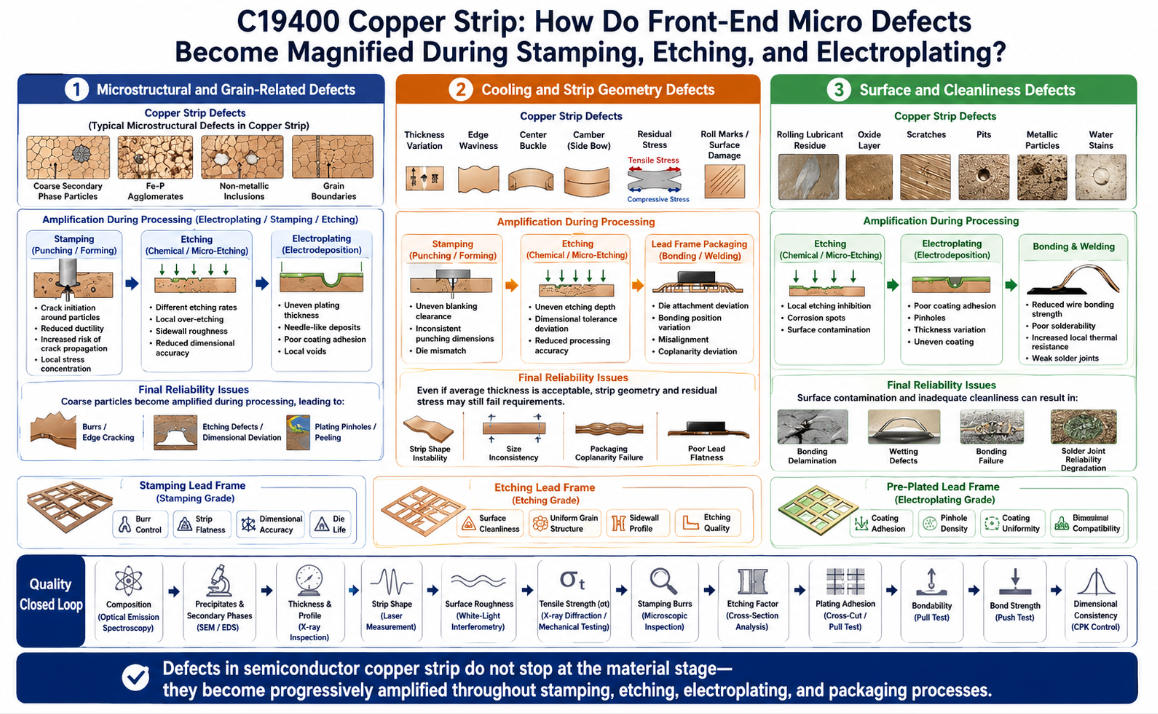
12. Final Acceptance Cannot Rely Only on Tensile Strength and Electrical Conductivity
Lead frame copper strips require at least four levels of evaluation:
| Evaluation Level | Key Items |
|---|
| Material level | Composition, inclusions, Fe-based particles, grain structure, texture, precipitation, and cleanliness |
| Copper strip level | Thickness, flatness, surface condition, hardness, tensile properties, electrical conductivity, residual stress, and slit edge quality |
| Processing level | Stamping burrs, feeding stability, etching factor, undercutting, plating adhesion, and soldering/bonding compatibility |
| Package level | Die bonding, wire bonding, molding, reflow, humidity-heat testing, temperature cycling, and lead coplanarity |
For wide and long coils, it is also necessary to establish maps of thickness, hardness, electrical conductivity, and residual stress at multiple positions including the head, middle, tail, and transverse directions. Reliable
copper strip suppliers should provide consistent quality data to support process evaluation. Average values can only indicate overall conditions, while minimum values and variation determine whether high-speed production lines can operate stably.
13. Conclusion: The “Metal Framework” of Chips Is Sold Through Coil-to-Coil Consistency
The manufacturing of C19400 lead frame copper strips is a continuous control chain from melt cleanliness to final package reliability. Melting and casting determine the limits of particles, inclusions, and segregation. Hot rolling and cold rolling determine thickness, texture, dislocation structure, and flatness. Annealing and precipitation control adjust strength, electrical conductivity, and residual stress. Leveling, slitting, and surface treatment determine whether the material can reliably enter stamping, etching, and electroplating processes.
A single coarse particle may create burrs during stamping; a rolling scratch may become a broken lead after etching; a section of copper strip with abnormal residual stress may suddenly warp after slitting or etching.
Therefore, the true challenge of lead frame copper strip manufacturing is not simply rolling C19400 to a sufficiently thin thickness. The real challenge is maintaining thickness, flatness, strength, electrical conductivity, surface quality, and residual stress within acceptable packaging process windows over thousands of meters of strip length.
References and Standards
The following references and standard materials are used to support the composition and product positioning of C19400, thermomechanical processing, residual stress, precipitation structures, etching behavior, and lead frame manufacturing. Actual products should be evaluated according to formal standards, supplier technical agreements, and package validation results.
[1] Copper Development Association. C19400 Alloy Profile and Fabrication Properties. Copper.org Alloy Database.
[2] ASTM International. ASTM B465-20, Standard Specification for Copper-Iron Alloy Plate, Sheet, Strip, and Rolled Bar.
[3] Aurubis. C19400 (CuFe2P) Copper Alloy Strip Data Sheet.
[4] Proterial Metals. Copper Alloy Strip for Semiconductor Lead Frames: C194 and Related Alloys.
[5] Mitsubishi Materials. TAMAC Series (Cu-Fe Alloy): C19400/TAMAC194 for Lead Frames and Electronic Parts.
[6] KME Germany. STOL 194—C19400/CuFe2P Engineering Copper Solutions Data Sheet.
[7] Fisk Alloy. C194 Copper-Iron (CuFe2P): Lead Frame and Connector Alloy Overview.
[8] First Copper Technology. Leadframe Copper Alloy C194 and C19210 Product Data.
[9] ASTM International. ASTM B888/B888M, Copper Alloy Strip for Use in Manufacture of Electrical Connectors or Spring Contacts.
[10] Cao T, Wang S, Zhao G, Wu X, Liaw P K, Qiao J. Evolution of Microstructure and Residual Stress for a Lead-Frame Cu-2.13Fe-0.026P Alloy. Journal of Alloys and Compounds, 2023: 171383. doi:10.1016/j.jallcom.2023.171383.
[11] Yang J, et al. Influence of Short-Time Annealing on the Evolution of the Microstructure, Mechanical Properties and Residual Stress of the C19400 Alloy Strips. Journal of Alloys and Compounds, 2023, 941: 168705. doi:10.1016/j.jallcom.2023.168705.
[12] Yang J, Bu K, Zhou Y, et al. Microstructure, Residual Stress, and Mechanical Properties Evolution of a Cu-Fe-P Alloy under Different Conditions. Journal of Materials Research and Technology, 2023, 24: 7896-7909. doi:10.1016/j.jmrt.2023.05.015.
[13] Zhou F, Zhang Y, Lu L, Song K, Gao H. Effects of a Thermal-Ultrasonic Stress Relaxation Process on the Residual Stress, Mechanical Properties and Microstructures of C19400 Copper Alloy Strips. Materials Science and Engineering A, 2022, 841: 143014. doi:10.1016/j.msea.2022.143014.
[14] Wang T, Hu L, Guo Y, et al. Microstructure Evolution in Cu-2.13Fe-0.026P (wt%): The Contribution of Texture Intensity to Residual Stress Variation. Journal of Alloys and Compounds, 2024, 1008: 176509. doi:10.1016/j.jallcom.2024.176509.
[15] Wang T, et al. Microstructure Evolution in Cu-2.13Fe-0.026P Alloy Strips: Annealing, Conductivity, Residual Stress and Etching Performance. Journal of Alloys and Compounds, 2024.
[16] Fang J, et al. Influence of Etchants on Etched Surfaces of High-Strength and High-Conductivity Copper Alloys for Lead Frames. Materials, 2024, 17(9): 1966.
[17] Yu Q, et al. Microstructure Evolution and Recrystallization Mechanisms of a Cu-Fe-P Alloy for Lead Frames. Materials, 2024, 17(9): 2015.
[18] Zhou Y, et al. Characterizations on Precipitations in the Cu-Rich Corner of Cu-Fe-P Based Lead Frame Alloys. Crystals, 2023, 13(2): 274.
[19] Chen X Z, Yang Y Z, Lin Q S, et al. Optimization of Thermomechanical Treatment and Properties of Cu-Fe-P Alloy C194. Advanced Materials Research, 2011, 415-417: 724-727.
[20] Yang C X, Guo F A, Xiang C J, et al. Microstructure and Properties of Aged Cu-Fe-P Alloy. Special Casting & Nonferrous Alloys, 2007, 27(12): 975-978.
[21] Liu R Q, Liu K, Xie S S, et al. Effect of Multi-Stage Aging on Properties of Hot-Rolled C194 Alloy. Chinese Journal of Rare Metals, 2006, 30(S1): 155-157.
[22] Liu J S, et al. Research Status of Preparation Technology of C19400 Alloy Strip for Lead Frames. Shanghai Nonferrous Metals, 2026.
[23] Precision Micro. The Economic Manufacture of Lead Frames: Stamping and Chemical Etching—Technical Comparison.
[24] Proterial Metals. Product Line-Up and Quality Requirements for Copper Alloy Strip for IC Lead Frames.
[25] Mitsubishi Materials. TAMAC Copper Alloy Series for Semiconductor Lead Frames, Power Semiconductors and Electronic Components.
[26] GB/T 20254.1. Copper and Copper Alloy Strip for Lead Frames—Part 1: General Requirements.
[27] JIS H 3110. Phosphor Bronze and Nickel Silver Sheets, Plates and Strips; related Japanese electronic copper strip specifications.
[28] EN 1652. Copper and Copper Alloys—Plate, Sheet, Strip and Circles for General Purposes.
[29] Research Progress of Cu-Ni-Si Series Alloys for Lead Frame Materials. Coatings, 2025, 15(1): 91.
[30] Research Status and Key Technology Analysis of Integrated Manufacturing of High-Precision Copper Alloy Strip for Lead Frames. 2022.

 English
 한국어
한국어 français
 Deutsch
 Español
 italiano
 العربية
 tiếng việt
 Türkçe
 ไทย
ไทย 中文
中文